Truenorth
intro of Truenorth
Truenorth is an efficient, scalable, and flexible non–von Neumann architecture inspired by the brain’s structure. It is a 5.4-billion-transistor chip with 4096 neurosynaptic cores interconnected via an intrachip network that integrates 1 million programmable spiking neurons and 256 million configurable synapses.
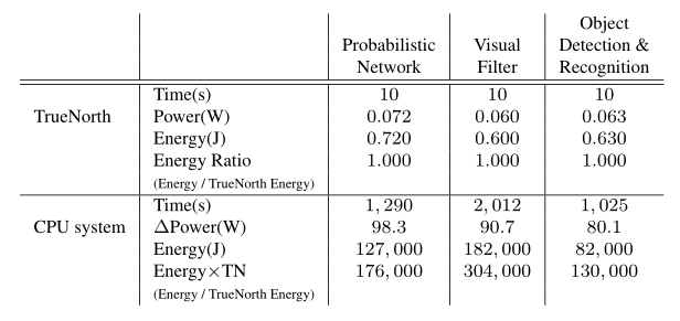
The architecture is well suited to many applications that use complex neural networks in real time, for example, multiobject detection and classification. With 400-pixel-by-240-pixel video input at 30 frames per second, the chip consumes 63 milliwatts.
von Neumann bottleneck
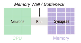
In terms of memory,the von Neumann bottleneck,which is caused by separation between the external memory and processor, leads to energy-hungry data movement when updating neuron states and when retrieving synapse states. In terms of communication, interprocessor messaging explodes when simulating highly interconnected networks that do not fit on a single processor.
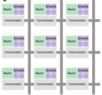
Conceptual blueprint of an architecture that, like the brain, tightly integrates memory, computation, and communication in distributed modules that operate in parallel and communicate via an event-driven network.
design of truenorth
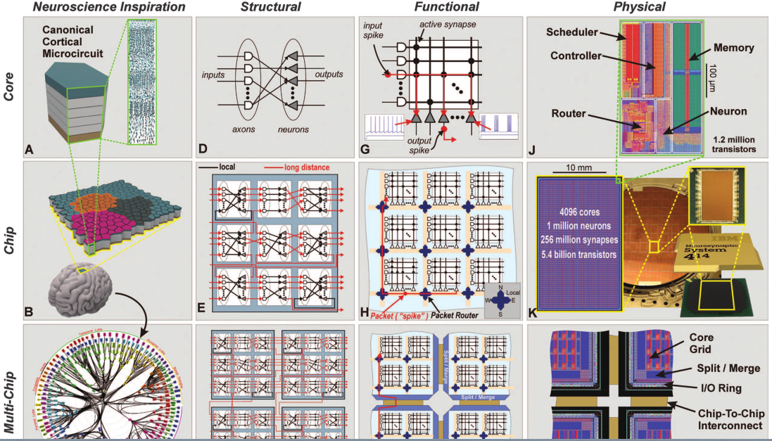
Structure of a neurosynaptic core with axons as inputs, neurons as outputs, and synapses as directed connections from axons to neurons.
Functional view of core as a crossbar where horizontal lines are axons,crosspoints are individually programmablesynapses,vertical lines are neuron inputs, and triangles are neurons. Information flows from axons via active synapses to neurons. Neuron behaviors are individually programable.
Functional chip architecture is a two-dimensional array of cores where long-range connections are implemented by sending spike events (packets) over a mesh routing network to activate a target axon. Axonal delay is implemented at the target.
Routing network extends across chip boundaries through peripheral merge and split blocks.
Physical layout of core in 28-nm CMOS fits in a 240-mm-by-390-mm footprint. A memory (static random-access memory) stores all the data for each neuron, a time-multiplexed neuron circuit updates neuron membrane potentials, a scheduler buffers incoming spike events to implement axonal delays, a router relays spike events, and an event-driven controller orchestrates the core’s operation.
critical details of truenorth
The neurosynaptic core includes 256 neurons (computation), 256 axons (communication), and 256 × 256 synapses (memory).
TrueNorth is a hybrid asynchronous-synchronous chip: the asynchronous control and communication circuits do not require a resource-intensive fast global clock, and the synchronous compute circuits operate only when necessary as they are “clocked” by the asynchronous control. The frequency of the clock is only 1kHz.
We implemented TrueNorth’s neurons using an all-digital approach.Our digital neuron uses time-division multiplexing, enabling us to amortize its area and leakage costs.
the neurons and synapses can exhibit pro-grammed stochastic behavior via a pseudo-random number generator (one per core).
high efficiency of truenorth
In terms of efficiency, TrueNorth’s power density is 20 mW per cm2,whereas that of a typical central prosessing unit(CPU) is 50 to 100 W per cm2.
Active power density was low because of our architecture, and passive power density was low because of process technology choice with low-leakage transistors.
For a typical network with neurons that fire at an average rate of 20Hz and make an average of 128 connections, a core will receive on average five incoming spike events in a 1ms time step, which corresponds to ∼640 neural updates. Out of the possible 256 × 256 (= 65,536) neural updates in the time step, our event-driven Controller only performs these ∼640 updates thereby eliminating 99% of the unnecessary circuit switching in the Neuron.
At the operating point where neurons fire on average at 20 Hz and have 128 active synapses, the total measured power was 72 mW (at 0.775 V operating voltage), corresponding to 26 pJ per synaptic event (considering total energy).Compared with anoptimized simulator running the exact same network on a modern general-purpose microprocessor,TrueNorth consumes 176,000 times less energy perevent.Compared with a state-of-the-art multiprocessor neuromorphic approach (48 chips each with 18 microprocessors)running a similar network,TrueNorth consumes 769 times less energy per event.
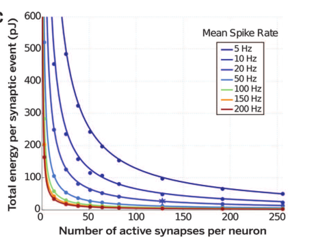
The total energy(passive plus active) per synaptic event decreases with higher synaptic density because leakage power and baseline core power are amortized over additional synapses.
test of truenorth
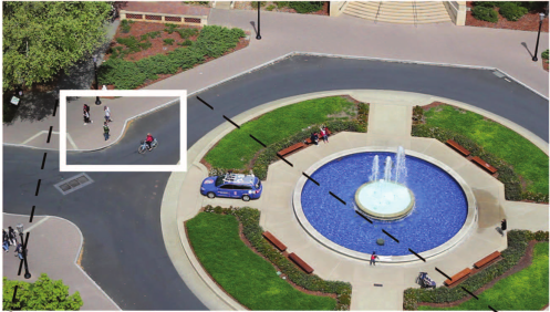
To test TrueNorth’s applicability to real world problems, we developed an additional multiobject detection and classification application in a fixed-camera setting.
The task had two challenges: (i) to detect people, bicyclists, cars, trucks, and buses that occur sparsely in imageswhileminimizingfalsedetectionand(ii) to correctly identify the object.
Operating on a 400-pixel-by-240-pixelaperture,thechipconsumed 63 mW on a 30-frame-per-second three-color video, which when scaled to a 1920-pixel-by-1080-pixel video achieved state-of-the-art performance.
